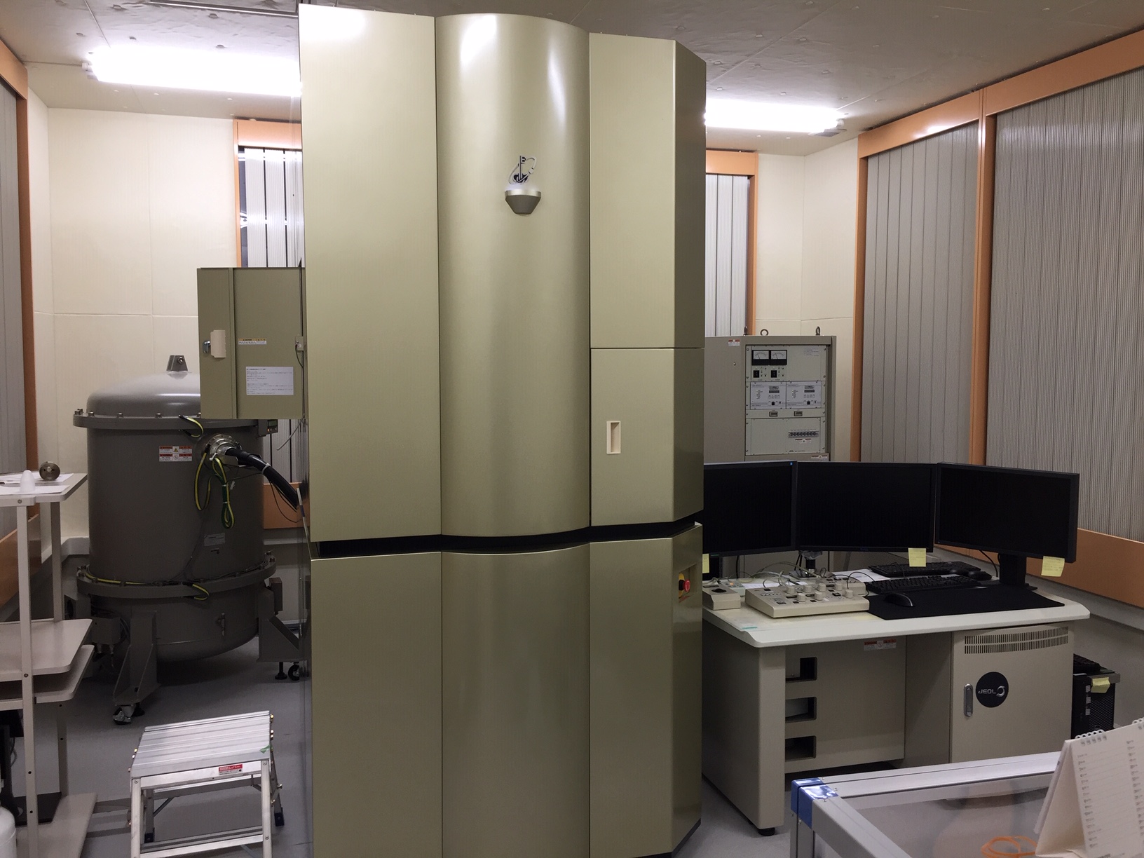
Field emission transmission electron microscopeTransmission electron microscope
Exterior
no image

no image
Overview
This is a field emission electron microscope manufactured by JEOL Ltd. Unlike conventional transmission electron microscopes (TEM), atomic images can be observed by operations similar to scanning electron microscopes (SEM). Scanning transmission imaging (STEM) is also possible, and it is possible to simultaneously acquire high-angle scattering dark-field images (HAADF-STEM), bright-field images (STEM-BF), and secondary electron images (SEI). It is also possible to obtain an elemental mapping image with the attached EDS (SDD).
| Name (abbreviation) | Field emission transmission electron microscope(FE-STEM) |
|---|---|
| Model number (manufacturer) | JEM-2800 (JEOL) |
| Electron gun | Schottky type |
| Accelerating voltage | 200kV, 100kV |
| Resolution | 0.1nm (transmission image TEM), 0.2nm (scanning image STEM), 0.5nm (secondary electron image SEI) (at 200kV) |
| EDS detector | Silicon drift detector(SDD)(100mm^2) |
| Sample holder | Beryllium 2-axis tilt holder, cooling (liquid nitrogen) 2-axis tilt holder |
| Installation location | Electron microscope room 2 (next to the west of Building C3) |
| Equipment manager | Department of Bio and Applied Chemistry Yoshihiro Kusano |
Contact us
Please feel free to contact us from the following.
