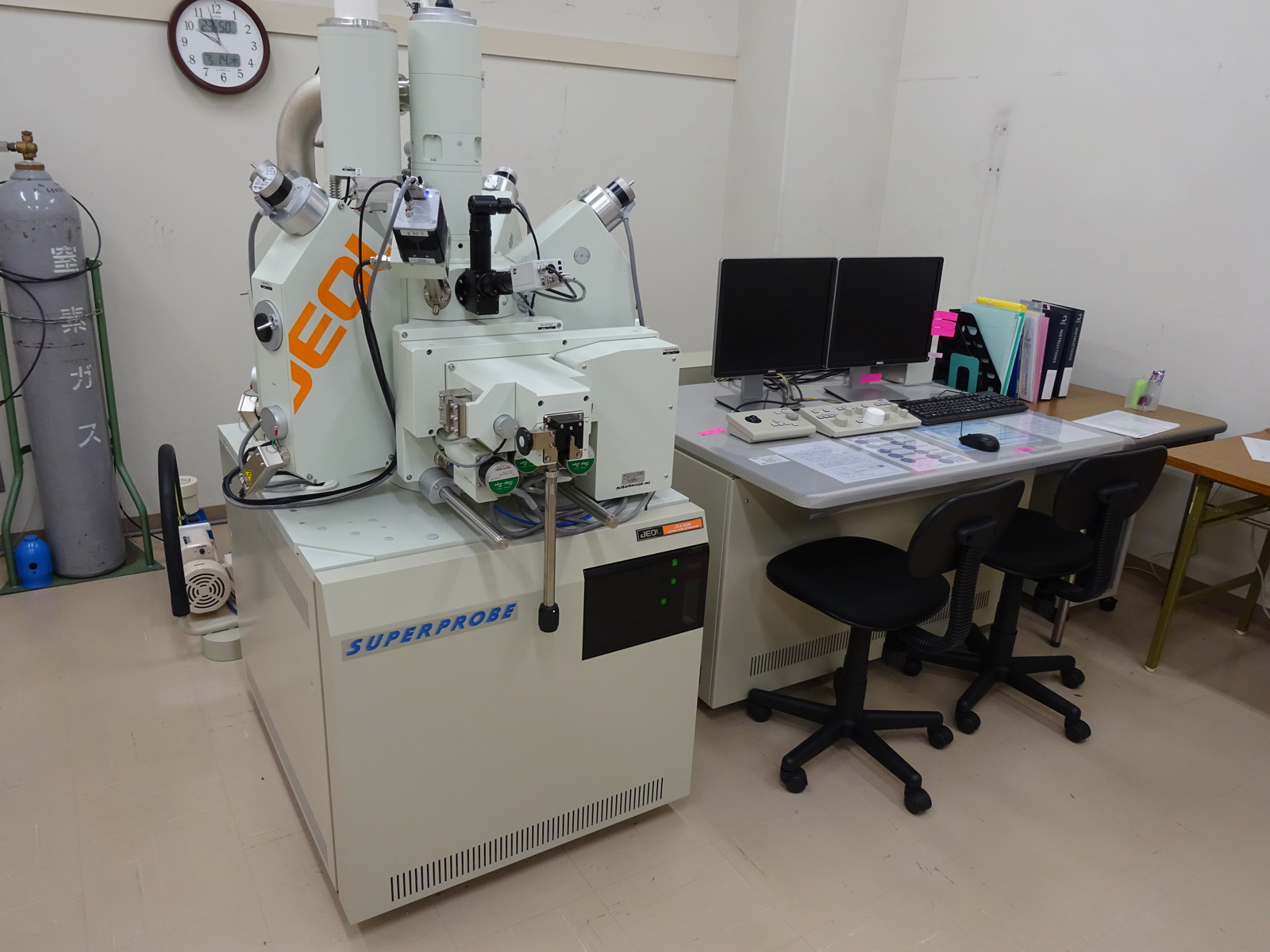
Electron probe surface analyzerElectron Prove Microanalyzer
Exterior
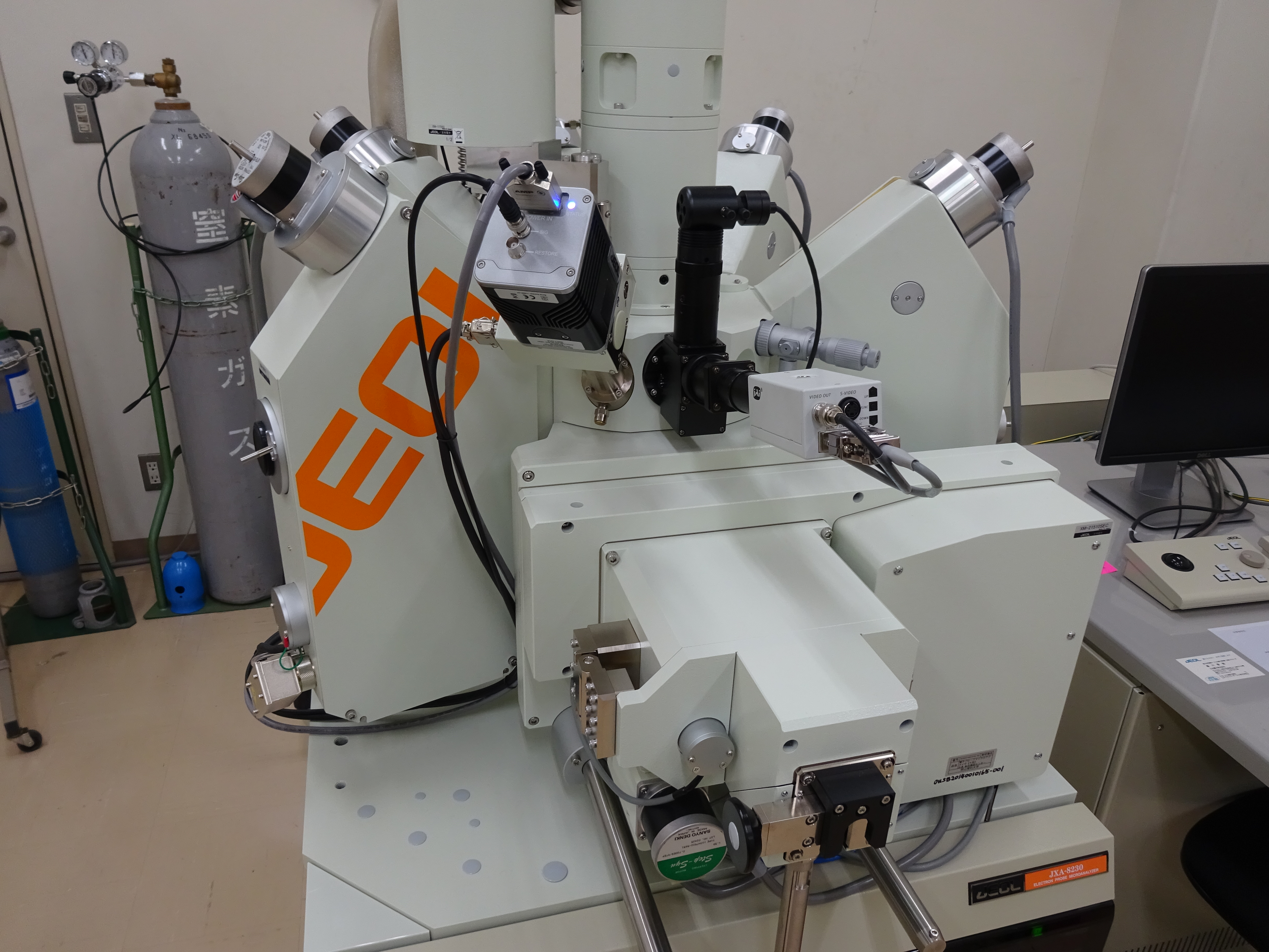
Goniometer part
no image

Overview
It is possible to perform elemental analysis of minute parts (μm order) while observing an electron microscope image (SEM). It can be displayed as a secondary density distribution color image (surface analysis) based on information such as characteristic X-rays from the sample and image signals (secondary electrons, reflected electrons). Qualitative analysis and semi-quantitative analysis using energy dispersive spectroscopy (EDS) are easy and the results can be obtained in real time. Due to its good position reproducibility, if the analysis position is preset and the analysis conditions are determined, a large number of analytical operations can be automatically performed from the workstation, quantitative analysis can be performed at high speed, and analysis data can be collected and processed.
| Name (abbreviation) | Electronic probe microanalyzer(WDS) |
|---|---|
| Name (abbreviation) | JXA-8230 (JEOL) |
| Elemental analysis range | 5B~92U |
| Accelerating voltage | 0.2~30kV |
| Secondary electron resolution | 6nm |
| Maximum magnification | 300,000 times |
| Observation image | Secondary electron image, Backscattered electron image, Topographic image, Composition image |
| Installation location | Room ⑤, 2nd floor, Building C3 |
| Equipment manager | Frontier Science and Engineering Laboratory Takeshi Imayama |
Contact us
Please feel free to contact us from the following.
