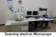
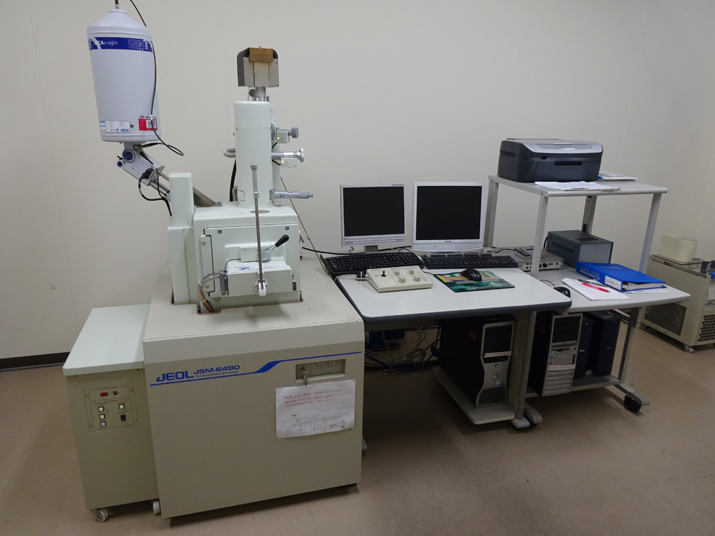
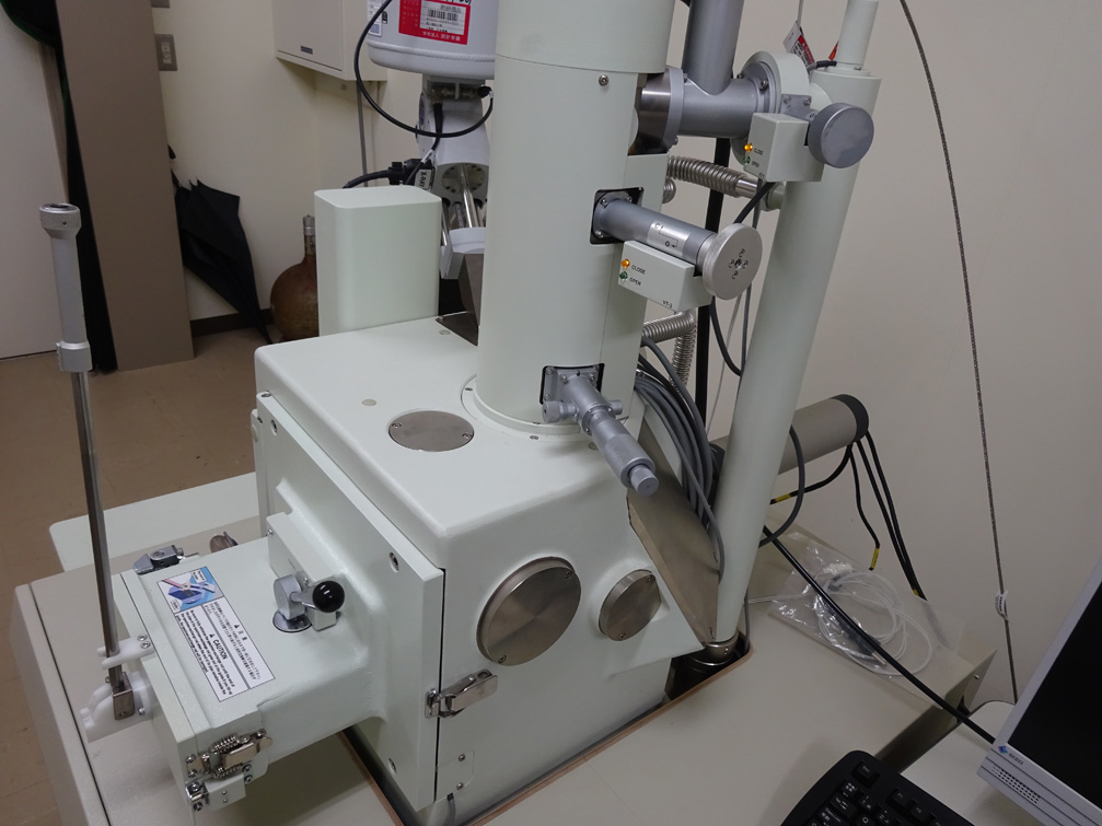
Scanning electron Microscope
OutlineOutline
Scanning electron microscope (SEM) is an equipment that can microscopically observe the surface of solids using electron beams. The samples that can be observed by SEM are metal, inorganic, and organic materials. In our SEM equipment (JSM-6490, JEOL), two kinds of images can be obtained for the microsurface of these solids. One is the secondary electron image that can be used when observing the surface morphology of a samples in the magnification ranges of 2000-10000 times. In the observation using the secondary electron image mode, it is usually observed without any special treatments for the samples possessed electrical conductivity such as metal samples. In contrast, for the observation using this mode for general inorganic and organic samples such ceramics and polymers, the samples should be coated by carbon and gold thin films because most of inorganic and organic materials have no electrical conductivity. Therefore, these samples are generally coated prior to the observation in order to make the sample electrically conductive. In this observation mode, qualitative and quantitate analyses of elements (except for H, He, Li and Be) on microscopic ranges are carried out by energy dispersive X-ray spectroscopy (EDS). These measurements also enable us to measure the concentration distribution of the element at the fine structure. Other is the backscattered electron image using reflected electrons that contains information on the surface morphology as well as information on the types of elements in the observation area. Therefore, this observation mode included an extremely effective image for confirming the element distribution. In this equipment, it is extremely easy to switch detectors between the secondary electron and the backscattered electron images. For a crystalline sample with a smooth metal surface, the electron back scattered diffraction (EBSD) pattern can be used to determine the type, orientation, and size of the crystals in the observation area. At this time, the elemental composition of the part to be observed is first determined by EDS, and then the type of crystal, orientation direction, and size are determined by using EBSD.

PerformancePerformance
| Name (abbreviation) | Scanning electron Microscope(SEM) |
| Model number (manufacturer) | JSM-6490 (JEOL) |
| Emission current: Magnification | x5~300000 times |
| Installation location | Room ⑯, Bldg. B1, 1st floor |
| Equipment manager | Yasushi Sato, Department of Chemistry, Faculty of Science |
| Contact us | Contact form is open 24 hours a day. Contact by telephone: Direct 086-256-8473 ext.3242 |

